


After a busy week spent traveling for work and a morning digging out from a surprise snowstorm, I had a great weekend with my family. It was Sunday night before I heated up the soldering iron and got down to business building the ProASIC 3 nano FPGA board.
I started with the toughest component, the FPGA. Its central location and low height means that I will have an easier time accessing it before other components are mounted. That is not likely to be a big problem for this board, with plenty of space around the chip, but I would still prefer not to have to work around the filter capacitors if I can avoid it. On the other hand, its 100 pins and 0.5 mm pin pitch makes it far and away the most difficult soldering job on the PCB.
Getting the FPGA placed was tougher than I expected. Pins a half a millimeter apart are about a quarter of a millimeter wide and need to be aligned even more finely. Getting them lined up on all four sides of the chip took plenty of patience. With the chip misaligned, the silver pins and gold circuit board pads brightly threw back the light from my magnifier, but as I carefully and gently slid the chip around, darkness would suddenly emerge as the pins and pads aligned and the dark purple PCB shone through. Then I would line up another side of the chip, only to see the first side gleaming its misalignment at me once again.
Eventually patience won out, and all four sides were lined up. I gingerly tacked two corners in place, checked the alignment again, and began to solder, starting with one of the corners I tacked. As the solder holding that corner liquefied, the chip turned and my careful alignment was lost. I removed the heat, the solder solidified, and I could see the mess I had made:
Solder wick will not fix it, because there is solder under the pins where solder wick will not go. The best option for removing the chip is hot air. Sadly, my built-in supply is inadequate for soldering duty, so I will have to borrow a heat gun or hot-air soldering rig.
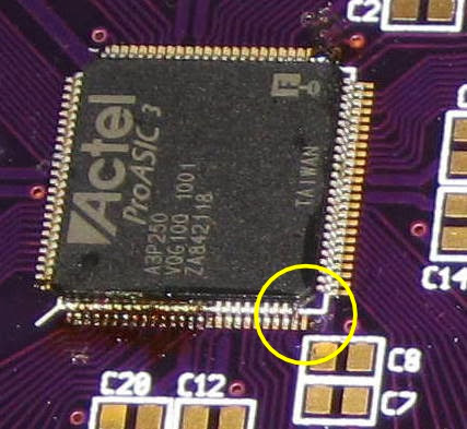
I like to follow the rule of never designing in a component I can not afford two of, so I started again with board number two and FPGA number two. After the requisite patient fiddling to get it all lined up, the soldering went smoothly, and I had a cleanly attached chip:

Some quick probing with an ohmmeter did not reveal any shorts between neighboring pins, but I need to make a thorough check and clean up the flux residue before I pronounce it done.
Laen’s PCB Order sent three boards, but for now I am keeping the third one in reserve. Mouser did not have the A3PN250 FPGA when I ordered parts, so I settled for the A3PN250Z, a lower-cost version that lacks Schmitt trigger inputs. Also, though I did not design the board with them in mind, there are other Actel Microsemi FPGAs with a similar pinout that may fit it. Leaving the third board unbuilt will keep my options open for later.
I have a few things on my agenda now. I think I know where I can borrow a heat gun, so with luck I can clean up the first board and recover its errant FPGA. Of course, I am also looking forward to mounting the rest of the parts on the second board and firing it up.
Look for a new feature on the blog next week. Until then, happy soldering!


0 comments:
Post a Comment